SEMICONDUCTOR ESD PROCESSING

Semiconductor ESD
Functional Surface Processing

From sample validation to repeatable production conditions.

Precision spray coating, dip coating and planar coating for semiconductor consumables, precision components, transparent substrates and complex workpieces.
PROCESS
Spray · Dip · Planar coating
SUBSTRATE
PET · PC · Engineering plastics · Metal
DELIVERY
Sample · Pilot · Production
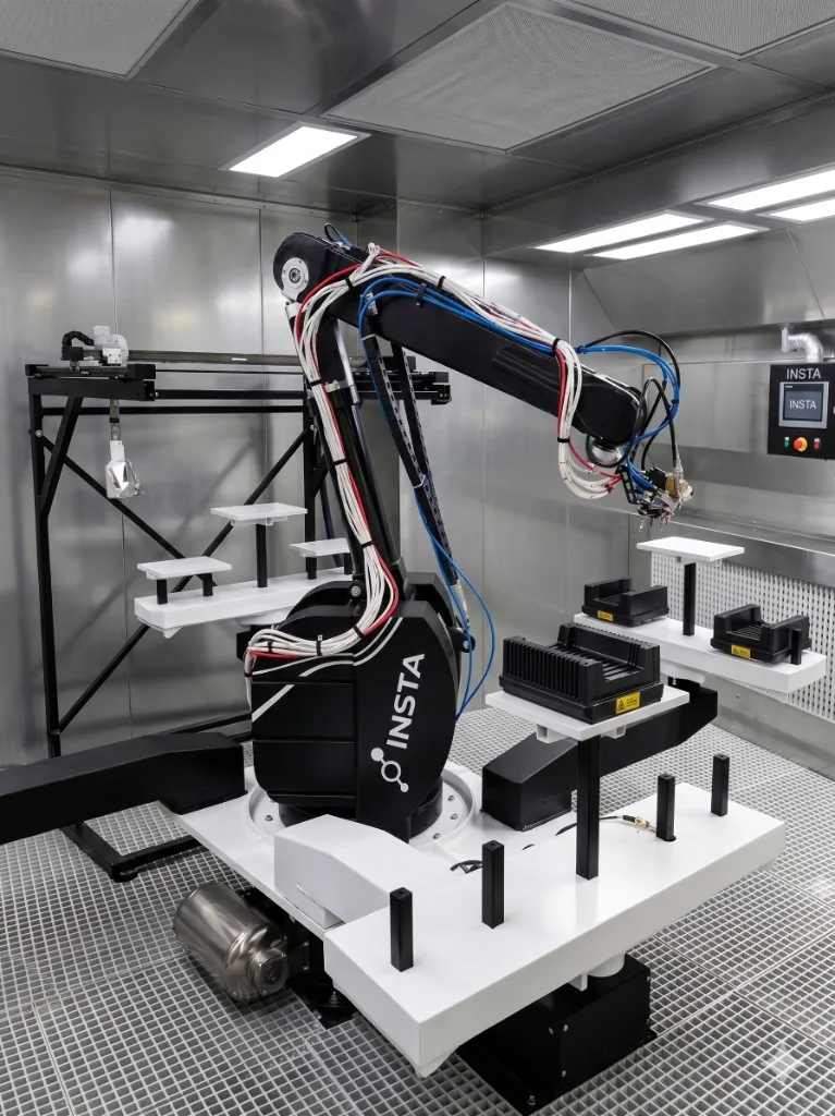
INSTA PRECISION automated spray coating equipment
AUTOMATED SPRAY COATINGAutomated Precision Coating

PROCESS ENGINEERING

Process Control &
Production Consistency

We define controls for surface resistance, appearance, adhesion and batch consistency around the substrate, pretreatment, coating, drying and fixture conditions. Sample approval and process records support repeatable production.

01

Performance

  • Surface resistance
  • Transparency & appearance
  • Contact angle
  • Adhesion
02

Process

  • Substrate pretreatment
  • Coating & film thickness
  • Drying & curing
  • Fixtures & masking
03

Production

  • Approved sample
  • Batch parameters
  • Inspection records
  • Clean packaging

CORE PROCESS

Three Processing Platforms

The process is selected around workpiece geometry, substrate behavior, target performance and acceptance criteria.

01 / SPRAYING3D

Precision Spray Coating

Functional coverage for complex geometry, corners and selected areas with controlled film thickness, coverage and surface resistance.

Workpieces
Wafer carriers, fixtures, equipment parts
Controls
Path, fixture, masking and drying
02 / DIP COATING360°

Dip Coating

Continuous coating of inner and outer surfaces, grooves and tubular structures for special geometries and batch processing.

Workpieces
Tubular and special components
Controls
Viscosity, withdrawal speed and drying
03 / PRECISION COATING2D

Planar Coating

Uniform antistatic coating for flat substrates with balanced transparency, appearance and batch stability.

Substrates
PET / PC film, carrier tape
Controls
Uniformity, thickness and curing

APPLICATION SYSTEM

Semiconductor & Precision Manufacturing

Functional surface processing for risks related to charge accumulation, particle attraction and surface failure.

Explore Applications
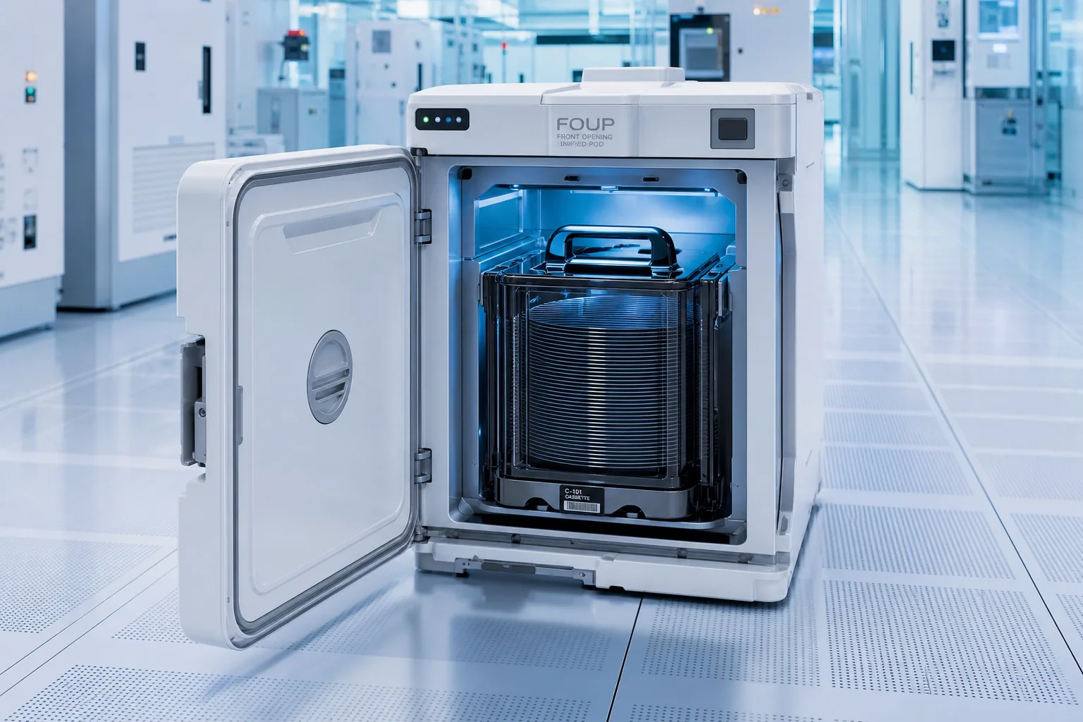
Semiconductor wafer carrier and clean-process application
01

Wafer Carriers

FOUP · FOSB · Cassette

02

Equipment & Fixtures

Engineering plastics · Precision parts

03

Electronic Packaging

IC Tray · Carrier Tape

04

Transparent Substrates

PET · PC · PMMA

PROCESS VALIDATION

From Specification to Production Baseline

Performance, appearance and process conditions are validated together to create a traceable project baseline.

VALIDATION FRAMEWORK

Production Validation

  1. 01Define requirements
  2. 02Record conditions
  3. 03Reproduce results
Quality Framework
01

Surface Resistance

Confirmed to project specifications

02

Contact Angle

Wetting and coating-property evaluation

03

Appearance & Adhesion

Haze, runs, scratches and adhesion

04

Safety Documents

SDS information aligned with GHS

PROJECT DELIVERY

Project Implementation Workflow

Requirements, process, validation and delivery conditions are established together.

INPUT
Substrate · Workpiece · Performance
OUTPUT
Process parameters · Acceptance baseline
  1. 01
    DefineMaterial · Geometry · Performance
  2. 02
    Select ProcessPretreatment · Coating · Drying
  3. 03
    Validate SampleAppearance · Resistance · Adhesion
  4. 04
    Pilot RunFixtures · Cycle · Packaging
  5. 05
    ProductionBatch parameters · Quality tracking

TECHNICAL INQUIRY

Start with the workpiece specification.

Share the substrate, drawing, target resistance, test method and estimated quantity.

Submit a Technical Request
+886 2 8686 0102+886 931 070 749