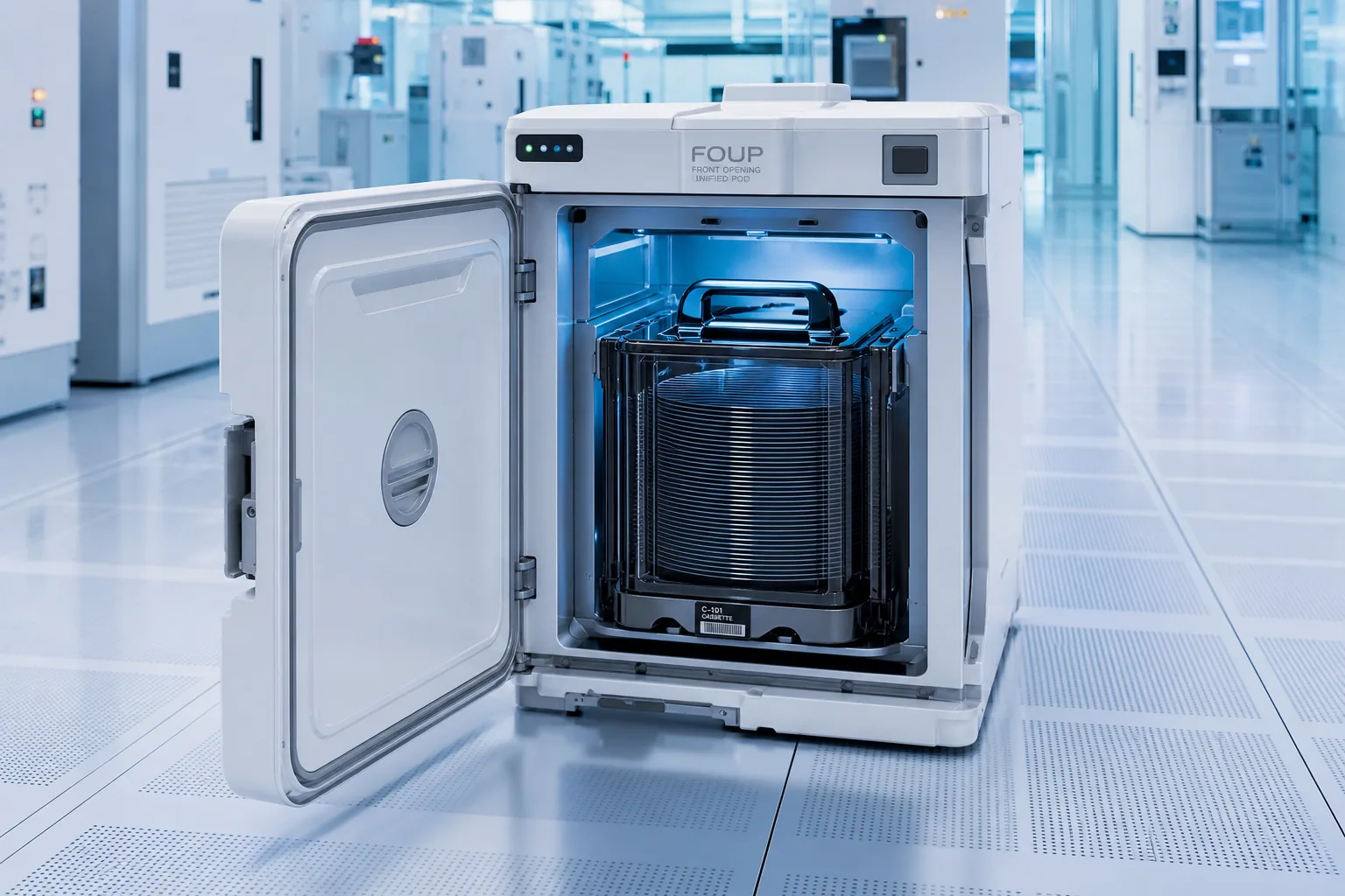
Wafer Carrier ESD Processing
Antistatic surface treatment for FOUP, FOSB and cassette systems to reduce particle attraction and electrostatic risk.
Our ESD processing solutions address dust attraction, discharge risk, haze, transparency loss and unstable production performance across diverse substrates.
Application-specific processing for semiconductor carriers, equipment consumables, automotive electronics and AI server components.
Antistatic surface treatment for FOUP, FOSB and cassette systems to reduce particle attraction and electrostatic risk.
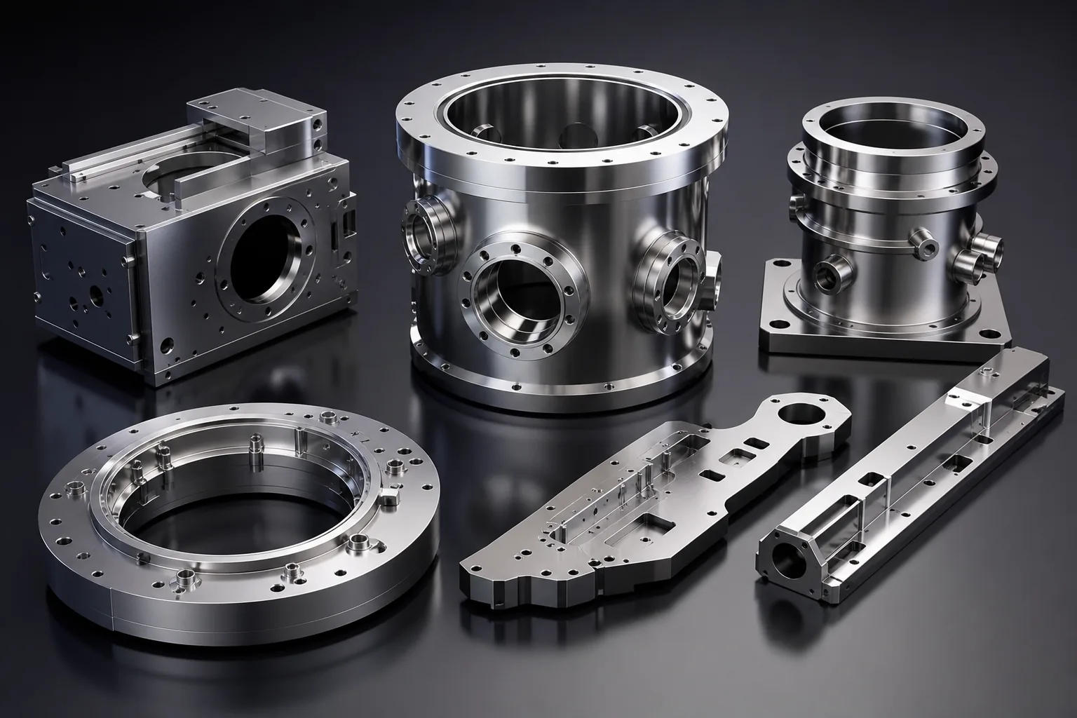
Surface treatment for components around CVD, PVD and etch equipment with attention to durability, cleanliness and maintenance risk.

Robot arms, EFEM contact surfaces, wafer-handling parts and cleaning fixtures processed to reduce friction dust and charge accumulation.

IC trays, carrier tape, conductive totes, dividers and packaging films for reduced triboelectric charging.
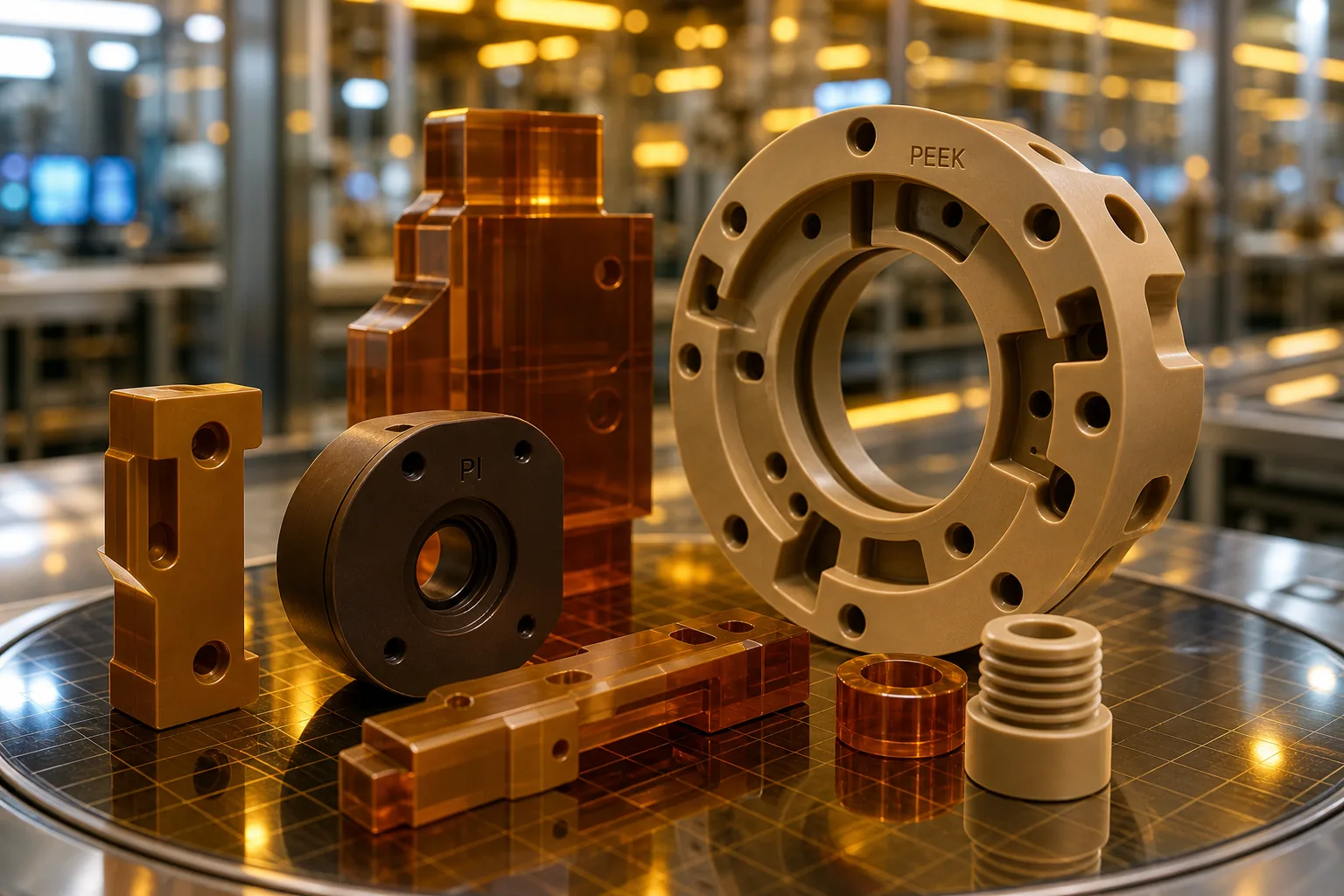
Precision processing and antistatic surface treatment for PEEK, PI, Vespel, PTFE and insulating consumables.
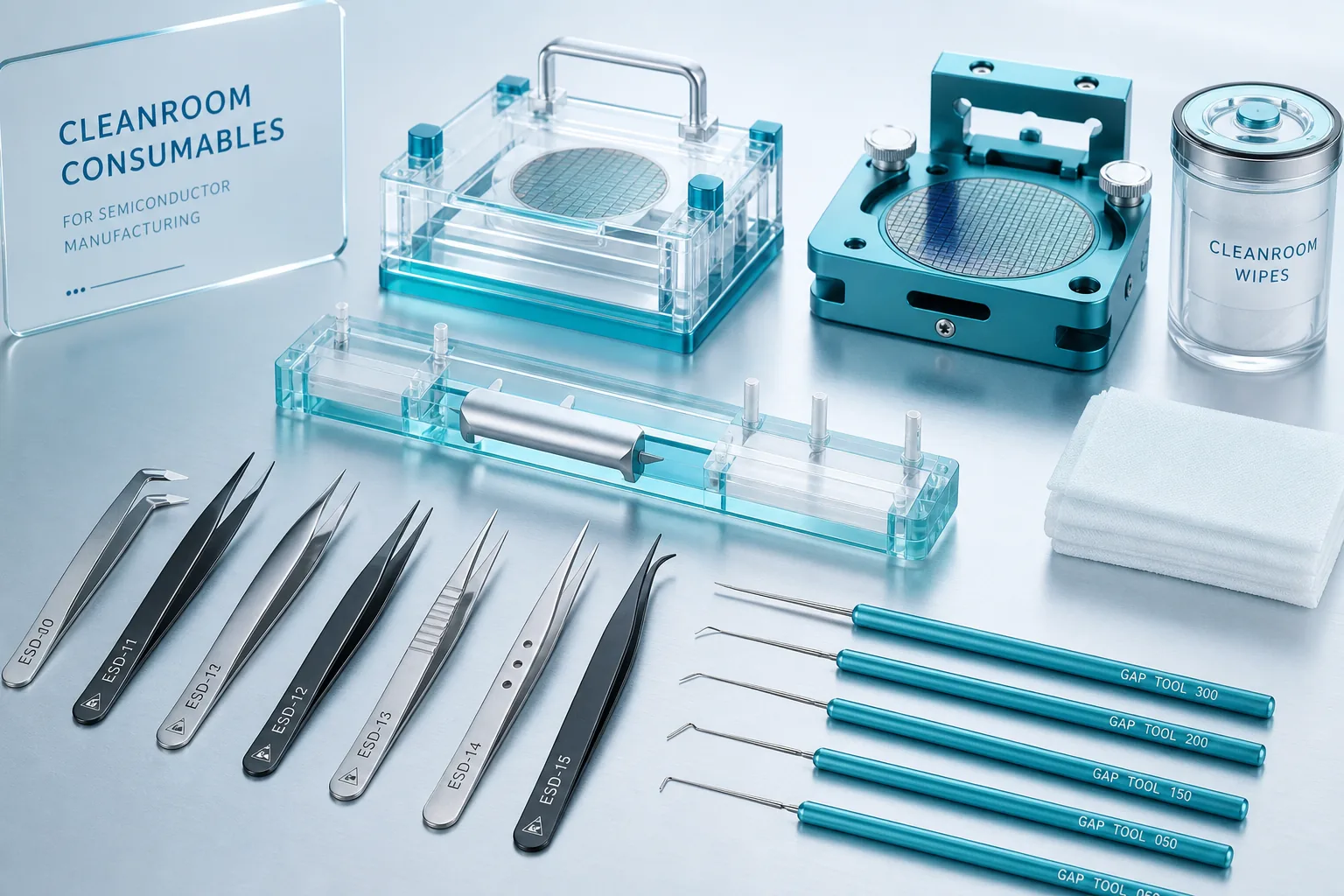
Custom gap tools, cleaning fixtures, wafer trays, clamps and production tools with low-dust antistatic surfaces.
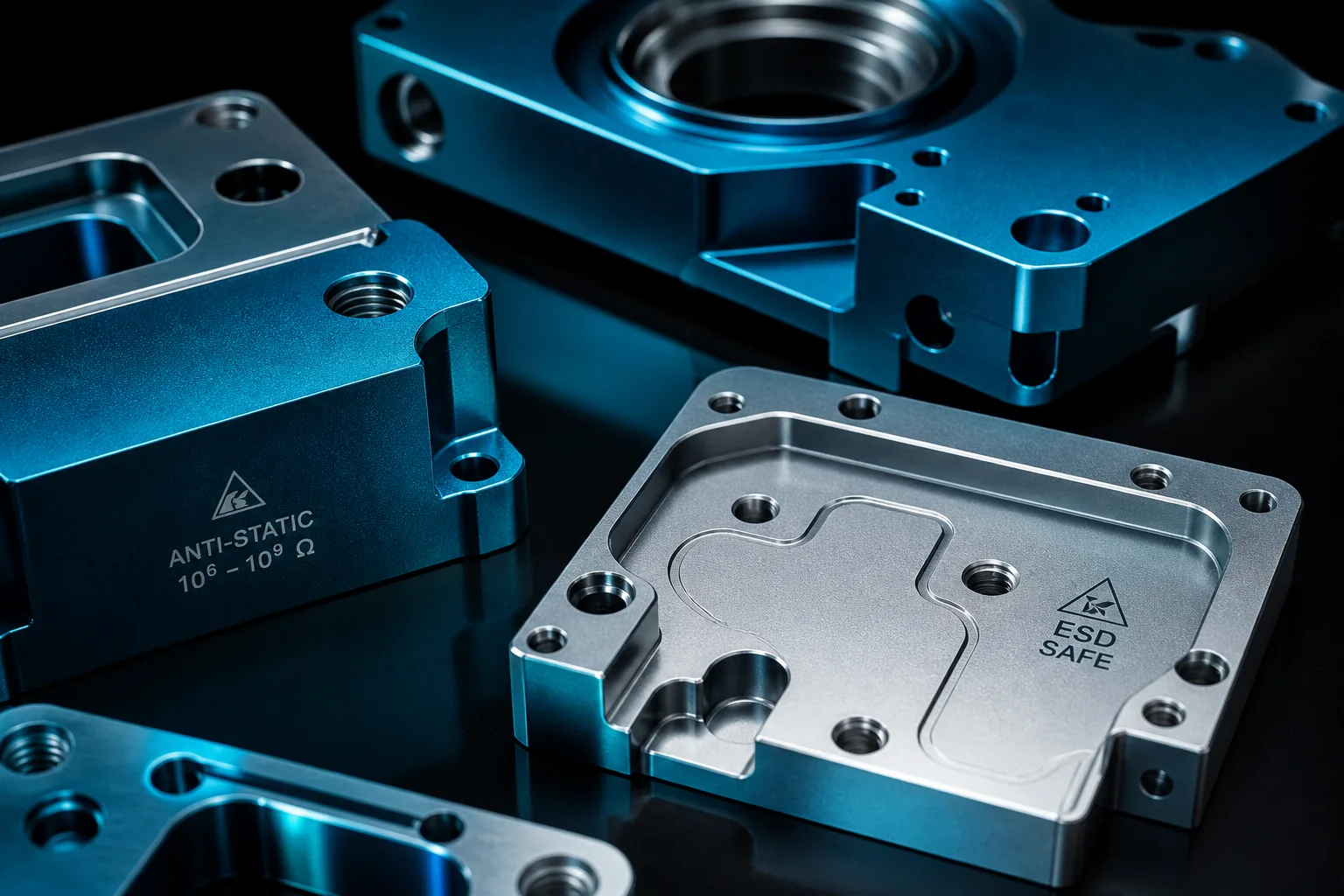
Post-process antistatic treatment for customer-supplied anodized aluminum cosmetic components, structures and housings. INSTA does not provide the anodizing step.
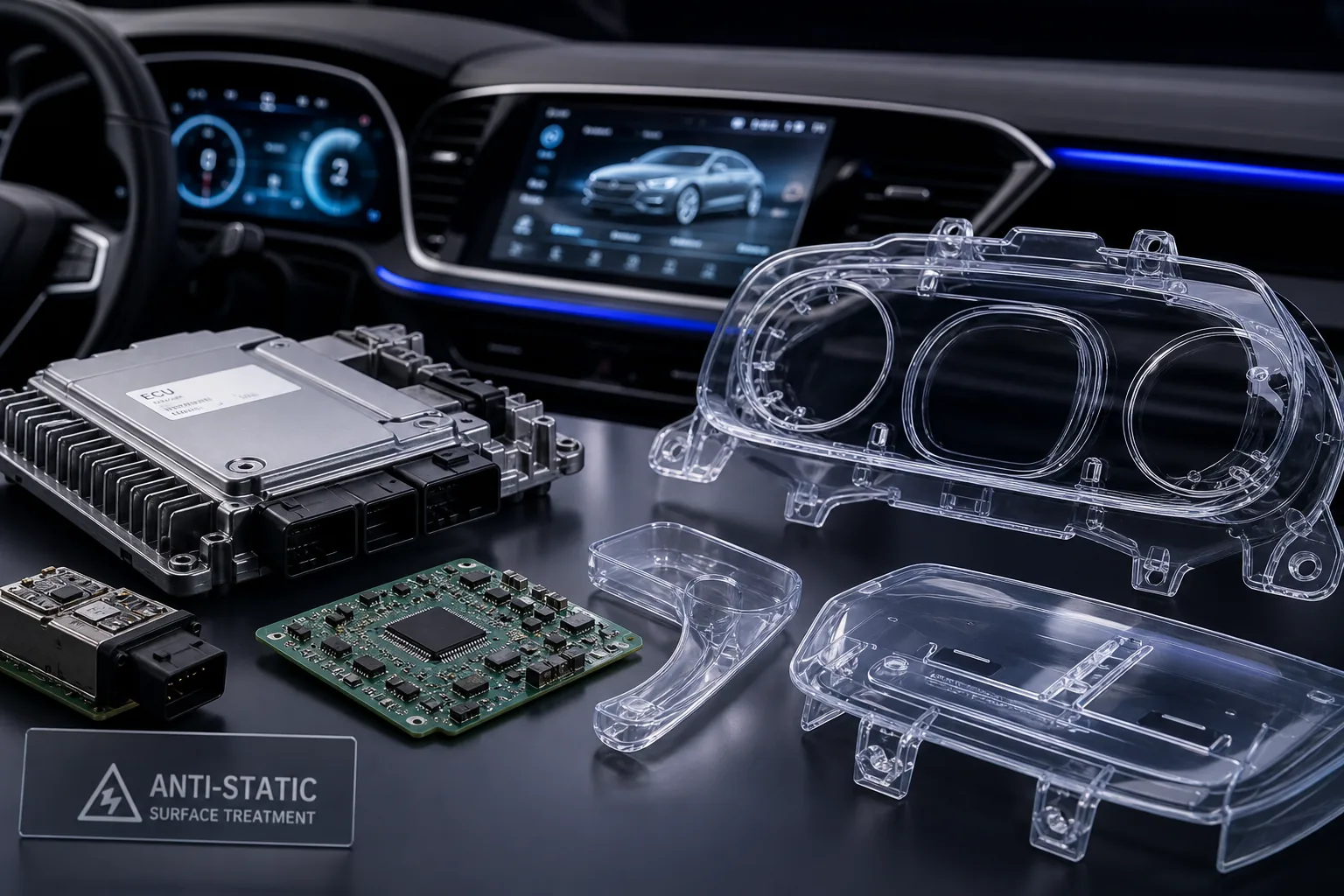
Automotive electronics, transparent interior parts, sensor surroundings and appearance-critical plastic components with reduced dust and static interference.
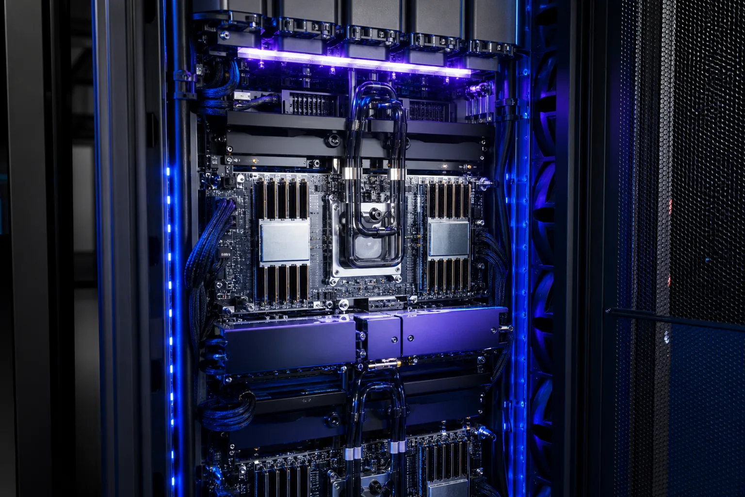
Surface treatment for server structures, electronic modules and thermal components to reduce dust attraction and charge accumulation.